I made a new backplane for my Terramaster F2-221 NAS
In a previous post I wrote about how I setup NixOS on my Terramaster F2-221 instead of using the included TOS provided by Terramaster. This in itself was quite simple as the NAS contains Intel J3355, a standard X86_64 CPU. However the NAS only has 2 SATA connectors, both of which were being used for the 4TB hard drives, so I had to resort to plugging in an external USB SSD for storing the operating system. This quickly became a little annoying to make room for this external SSD behind the NAS and make sure it's always plugged in when something is moved around in the shelf where I keep it, so I wanted to see if I could come up with a better solution.
Essentially what I wanted was this:
Researching my options
First I need to get out of the way the fact that there is an internal USB connector on the motherboard that contains a USB stick that ships with the NAS, that is used for downloading and bootstrapping TOS onto the storage drives. This USB header is only USB 2.0 though so it's not an option for this purpose.
Back when I first got the NAS I did add an extra RAM stick in the single RAM slot on the motherboard and I remembered seeing a PCIe (PCI Express) x4 connector on the motherboard that the backplane PCB connects into. As I recently got interested in designing PCBs I thought it might be interesting to see if I could come up with something, but when inspecting the existing backplane I noticed that there was no IC (integrated circuit) on there converting PCIe to SATA, instead it only contained some power circuitry and the SATA connectors were wired directly to the PCIe edge connector. This was a non-standard pinout and not PCIe at all, no room for expansion! But hey! This generation of NASes from Terramaster also include 4 and 5-bay units, how do they do that? Looking at the specs for Intel J3355 I could see that the CPU has 2 SATA ports and 6 lanes of PCIe gen 2 which would mean that the other models must be utilizing those PCIe lanes somehow to expand the number of SATA ports.
What followed was days of me scouring image search on duckduckgo and google to try to find high resolution pictures of the backplane PCB from either the 4 or 5-bay model.
Reverse engineering
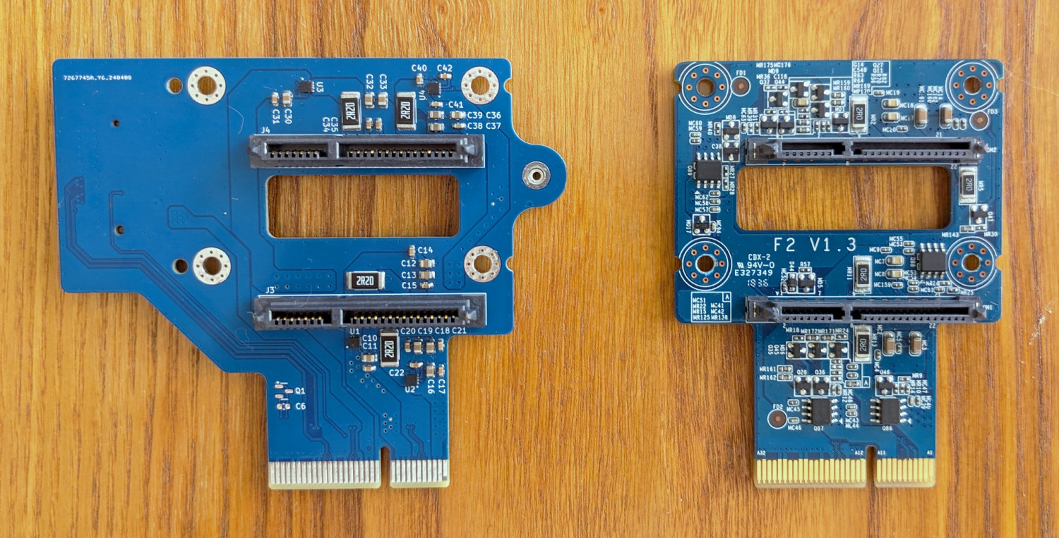
I found some great pictures from this review of Terramaster F5-422 and from those pictures I could identify that they're using 2 ASMedia ASM1061 ICs to get the SATA port count from 2 to 5. After some research I found out that ASM1061 is a 1-lane PCIe gen 2 SATA controller with 2 SATA ports, the first one is wired to port 3 and 4 on the backplane and the second one is wired to port 5 only. This was potentially good news for me as this means that the PCIe connector on the motherboard should include 2 PCIe x1 interfaces and looking at the back of the motherboard on my Terramaster F2-221 I could see that the pins that seemed to carry the PCIe traces on the F5-422 backplane were indeed wired up and it makes sense that they didn't want to have to manufacture different motherboards for the different models.
Quite a few differential pairs can be seen in this picture.
PCI Express
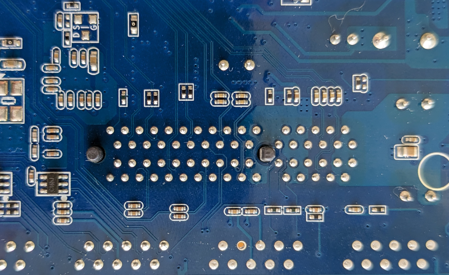
Some of the pictures were still a bit low resolution and I had to zoom in a lot and follow blurry traces but I could verify that the traces for the first 2 SATA ports matched the pins on my backplane PCB. Thankfully I could find a datasheet for ASM1061, and therefor had a pinout for the IC, so I knew which pins were the PCIe lines but all the differential pairs near the ICs and the PCIe connector went to vias and were then routed on internal layers which made it impossible for me to know for sure which differential pair was TX, RX
and REFCLK. I could however identify that one pin on the PCIe connector was connected to PERST#
on the ASM1061 ICs, that's something!
During this time I did some very extensive research into PCI Express routing and how it works and got a lot of small tidbits from here and there online and there was especially one little information that helped me with identifying the different differential pairs. That is that traditionally the TX
differential pair should have coupling capacitors, meaning that that the differential pair that connects to the TX
pins on the ASM1061 should have coupling capacitors on the backplane, but that is the RX
differential pair from the perspective of the CPU (and therefor the motherboard) and the differential pair connecting to the RX
pins on the ASM1061 IC should then have coupling capacitors on the motherboard side of the PCIe connector. Then looking at the pictures of the backplane PCB for F5-422 and the back of my motherboard I can identify the pins that have these coupling capacitors on the traces. After that only the REFCLK
remained and through guessing I was fairly confident that the closest differential pair to the TX
and RX
of each PCIe x1 interface was the REFCLK
for that interface.
And that left me with this pinout:
| B | A | |
|---|---|---|
| 1 | 12V | ? |
| 2 | 12V | 12V |
| 3 | 12V | 12V |
| 4 | GND | GND |
| 5 | SATA1 A+ | SATA1 B+ |
| 6 | SATA1 A- | SATA1 B- |
| 7 | GND | NC |
| 8 | 5V | 5V |
| 9 | 5V | 5V |
| 10 | ? | 5V |
| 11 | ? | ? |
| Notch | ||
| 12 | 3.3V | GND |
| 13 | GND | 3.3V |
| 14 | SATA2 A+ | 3.3V |
| 15 | SATA2 A- | GND |
| 16 | GND | SATA2 B+ |
| 17 | PERST# | SATA2 B- |
| 18 | GND | GND |
| 19 | PCIe1 TX+ | NC |
| 20 | PCIe1 TX- | GND |
| 21 | GND | PCIe1 RX+ |
| 22 | GND | PCIe1 RX- |
| 23 | PCIe1 REFCLK+ | GND |
| 24 | PCIe1 REFCLK- | GND |
| 25 | GND | PCIe2 RX+ 1 |
| 26 | GND | PCIe2 RX- 1 |
| 27 | PCIe2 TX+ 1 | GND |
| 28 | PCIe2 TX- 1 | GND |
| 29 | GND | PCIe2 REFCLK+ 1 |
| 30 | ? | PCIe2 REFCLK- 1 |
| 31 | ? | GND |
| 32 | GND | ? |
After having figured out this pinout I roughly verified the pinout of PCIe1 by bringing a picture of the F5-422 backplane into Kicad and routing the external traces to the vias that I can see and then attempt to route them on an internal layer, then assume I was incorrect in my pinout and attempt to route different combinations. My initial guess was the one that was easiest to route between the vias so I was fairly (-ish) confident in that I was correct.
You may also have noticed that some of the pins are marked
?. Most of these pins were not connected on my backplane and/or I could not figure out where they were routed to as those were also mostly routed on internal layers.
Power circuits
As stated earlier, there are no ICs on the F2-221's backplane that handle any PCIe signals, but one side of the PCB is full of components. After taking close-up pictures of the PCB so that I could identify the components and see where the traces go between them I recreated the schematic in Kicad. This circuit consisted of mostly mostfets, diodes, resistors and capacitors. Now, I am no electrical engineer but after staring at the schematic, trying to break it apart into chunks to make sense of it and doing a lot of research online I somehow figured that these were load switches with a slow starter, one for each power rail on each SATA port (meaning 4 load switches on F2-221 and 10 on the F5-422). One of the ground pins (P4) on the SATA connectors was also used as the enable pin for these load switches, as it's pulled to ground by the hard drive when connected. I figured this was done in combination with the slow start circuit to make hot-plugging the hard drives safe by preventing sparking across the connector and the drive due to the high initial inrush current.
Not being too eager to solder all these discrete components on my backplane PCB, I decided to find a complete integrated load switch IC with a built-in slow starter and finally went with the onsemi NCP45521-L.
Prototype
At this point I had spent a lot of time figuring out the pinout of the connector, and especially trying to figure out the purpose of the different unknown pins on the connector. And I figured it was time to just create a prototype PCB by routing what I did know and then breaking most of the other pins to test points that I can probe and try to figure out the purpose of.
SSD selection
Since beginning this process I had mostly been concerned with what would be possible and not what kind of boot SSD I wanted. Initially I wondered if I could add a SATA port by incorporating the same ASM1061 IC and then taping a SATA SSD somewhere inside the case. Then I had the ~~brilliant~~ obvious idea of trying to fit an M.2 connector on there, and as luck would have it there was just enough room for the connector between the mounting rails that the backplane screws into, and by just enough I mean there's less than a millimeter on each side!
As mentioned earlier, the CPU only has 2 SATA ports built-in and they are both being used for the 2 hard drives in the NAS. To get more SATA ports we'd need to get a controller that can convert some protocol into SATA, e.g. in external hard drive enclosures there is a controller that can communicate with the host over USB and the hard drive or SSD over SATA, and as I have 1 lane of PCIe I could use the same ASM1061 as Terramaster uses on the F5-422 to get 2 extra SATA ports and wire it up to an M or B-key M.2 slot for a SATA M.2 SSD. The biggest problem with this approach is that I can't just buy an ASM1061 and would instead need to buy a whole PCIe card containing an ASM1061 and extract the IC using a hot air station.
NVMe on the other hand is PCIe and no extra controller is needed, just wire the PCIe lines directly to the M-key M.2 slot and insert an SSD. This makes the PCB routing much simpler and costs less as we don't need to source any extra controller and there is more options for NVMe SSDs than SATA M.2 available. NVMe SSDs generally have 4 lanes of PCIe gen 3 or higher so in a way we're "wasting" 3 lanes and capping the 1 lane we do have to gen 2 speeds which in the end will not be faster that SATA speeds, but even taking that into account it makes no sense to go with anything else as it's cheaper and simpler for our use case. I ended up grabbing a Patriot P300 128GB for only €14.90 locally, that's cheaper than I could find a PCIe card with an ASM1061 IC.
I did however have some concern with if the BIOS would support booting directly from an NVMe drive, but then decided I would be ok with having an internal USB 2.0 usb stick to store the boot partition in the worst case.
Designing the prototype PCB
Even though I was creating my own PCB I was constrained with the mounting hardware that attaches the backplane to the case. Screw holes had to be positioned quite strictly in relation to the PCIe edge connector and the PCB had some restrictions for size and shouldn't restrict airflow too much. For those reasons, this prototype was also important for verifying that everything fits nicely in the case.
I first measured all different parts of the PCB using a ruler and calipers and then took a picture of the PCB as straight on as I possibly could and then tried to remove any lens distortion before importing the picture into Kicad and start positioning the PCIe connector, screw holes and the outline from the measurements and checking alignment with the picture. Then I made the schematic for the different components and layed them out on the PCB as best I could, but I wasn't too careful about placement as I knew this was only a temporary prototype and added testpoints for various pins. I discovered the 3.3V rail on the PCIe connector pretty late in this process and therefor there is a buck converter taking 5V and converting it to 3.3V for the NVMe SSD.
I sent my design to JLCPCB, ordered a 4-layer PCB and a couple of weeks later I had this!
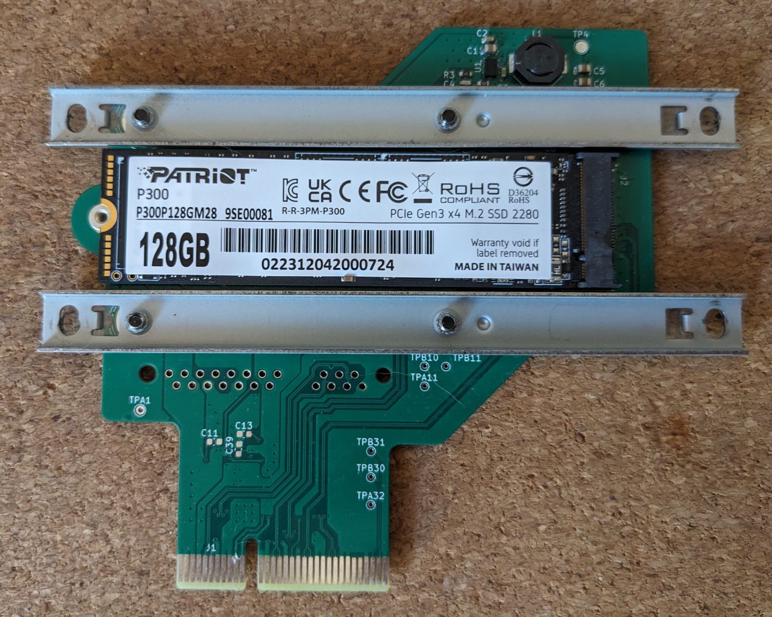
It's a bit of a weird shape because of the buck converter on the top right but look at how perfectly the SSD fits!
Testing the prototype PCB
This was my first time soldering DFN packages and they're tiny! Because I don't have a microscope or anything to visually inspect my soldering and these components were mostly just handling power anyway I just checked for shorts between power and ground and tried to take close-ups using my phone to see if I could spot any shorts. The technique that ended up working well for me to solder on these DFN packages without a stencil is to put what can only be described as way too much solder paste on the pads and then pushing the IC in the pool of solder, when the solder melts from the heat of my hot air station the IC will float on top and then I push down on it with tweezers and all excess solder will squeeze out and bead up, hopefully landing somewhere on the solder mask, where I can pick it up later once it's solid.
After a few attempts of successfully soldering all the ICs and the pins of the M.2 connector and actually plugging it into the motherboard, I booted it and there it was in the list of boot options, Patriot P300 128GB! It works! And I can boot from it directly!
My main concern before getting this prototype was that I still hadn't identified where to get the CLKREQ
line for PCIe1 and without it there wouldn't be any reference clock (REFCLK) active. When wiring up M.2 NVMe SSDs, the CLKREQ
line is usually pulled high using a resistor and then wired to the M.2 connector and the SSD will pull it low to request the reference clock when needed. This is done to save power and is part of PCIe Active State Power Management (ASPM). Luckily for me it seems that this line is permanently pulled low somewhere on the motherboard and may or may not be one of the pins broken out on the PCIe connector, but it doesn't really matter as I don't really need it! Yes, ASPM will not work but this is a boot drive for an always on server so who cares!
I also plugged in the hard drives and not as surprisingly they worked fine too!
So the prototype that I made as a last resort to be able to probe and debug actually just worked perfectly already and I don't care too much what the unidentified pins do anymore. If anyone does know or has a F5-422 and a multi-meter to figure it out, please let me know, but eh! ¯\_(ツ)_/¯
Moving on to V1.0
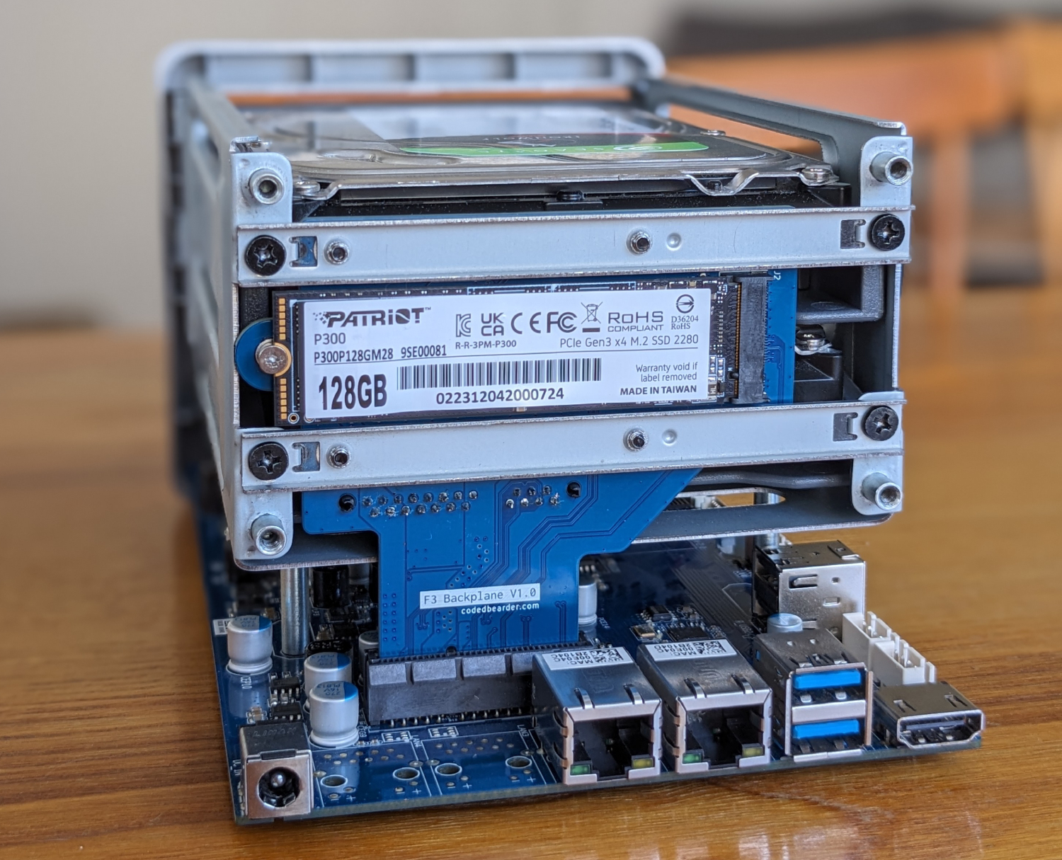
Even though the prototype worked perfectly fine, that being the end of the story with all the test points and having it sitting slightly crooked in the case (not to mention GREEN!), wasn't quite as satisfying as making a polished and final revision. There isn't much more to say about this one, I removed the buck converter and wired the M.2 connector directly to the 3.3V rail on the PCIe connector, adjusted positioning slightly to (hopefully) fix the slight crookedness of the prototype, removed the test points and slapped on a logo! I called it F3 Backplane because, you know, F2+1 :D
After ordering this new version from JLCPCB again and waiting another few weeks I received the final version of PCBs, soldered it up and tested it in the NAS and not so surprisingly this time it worked just as well as the prototype. I've done a full btrfs scrub of the hard drives to see if any errors arise, which they didn't and I've been running the system from the NVMe SSD for a few weeks now without any hiccups.
So you don't need to scroll up again here's a picture of the final version!
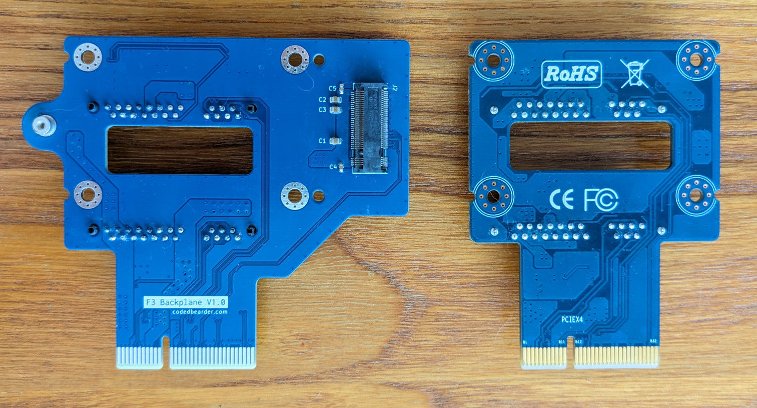
The soldering of the SATA connectors is kind of rough because I had forgotten to add thermal reliefs to the internal ground plane, making soldering very difficult. This has been fixed in the GitHub repository.
hdparm test results for the NVMe SSD:
/dev/nvme0n1:
 Timing cached reads:   4554 MB in  2.00 seconds = 2279.68 MB/sec
 Timing buffered disk reads: 1222 MB in  3.00 seconds = 407.22 MB/sec
This isn't very fast for an NVMe SSD but this is expected as it's only using 1 lane of PCIe gen 2. This is however totally fine for my use case.
Conclusion
All in all getting to this point was a lot of work and I learned a ton and I'm very happy with the results. I have made the Kicad project available on GitHub and hopefully it is useful to someone else too.
Discuss on Hacker News or Reddit